- 您现在的位置:买卖IC网 > Sheet目录39249 > LM4882MM/NOPB (NATIONAL SEMICONDUCTOR CORP) 0.48 W, 1 CHANNEL, AUDIO AMPLIFIER, PDSO8
Application Information (Continued)
device or the shutdown function may cause the “click and
pop” circuitry to not operate fully, resulting in increased “click
and pop” noise.
The value of C
i will also reflect turn-on pops. Clearly, a
certain size for C
i is needed to couple in low frequencies
without excessive attenuation. But in many cases, the
speakers used in portable systems have little ability to repro-
duce signals below 100 Hz to 150 Hz. In this case, using a
large input and output coupling capacitor may not increase
system performance. In most cases, choosing a small value
of C
i in the range of 0.1 F to 0.33 F, along with CB equal to
1.0 F should produce a virtually clickless and popless turn-
on. In cases where C
i is larger than 0.33 F, it may be
advantageous to increase the value of C
B. Again, it should
be understood that increasing the value of C
B will reduce the
“clicks and pops” at the expense of a longer device turn-on
time.
AUDIO POWER AMPLIFIER DESIGN
Design a 250 mW/8
Audio Amplifier
Given:
Power Output
250 mWrms
Load Impedance
8
Input Level
1 Vrms (max)
Input Impedance
20 k
Bandwidth
100 Hz–20 kHz ± 0.50 dB
A designer must first determine the needed supply rail to
obtain the specified output power. Calculating the required
supply rail involves knowing two parameters, V
OPEAK and
also the dropout voltage. The latter is typically 530mV and
can be found from the graphs in the Typical Performance
Characteristics. V
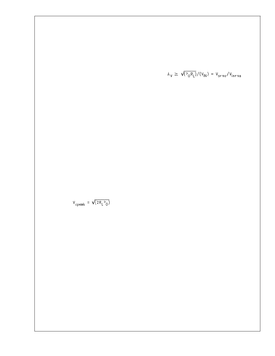
OPEAK can be determined from Equation
3.
(3)
For 250 mW of output power into an 8
load, the required
V
OPEAK is 2 volts. A minimum supply rail of 4.55V results
from adding V
OPEAK and VOD. Since 5V is a standard supply
voltage in most applications, it is chosen for the supply rail.
Extra supply voltage creates headroom that allows the
LM4882 to reproduce peaks in excess of 300 mW without
clipping the signal. At this time, the designer must make sure
that the power supply choice along with the output imped-
ance does not violate the conditions explained in the Power
Dissipation section.
Once the power dissipation equations have been addressed,
the required gain can be determined from Equation 4.
(4)
A
V =Rf /Ri
(5)
From Equation 4, the minimum gain is:
A
V = 1.4
Since the desired input impedance was 20 k
, and with a
gain of 1.4, a value of 28 k
is designated for R
f, assuming
5% tolerance resistors. This combination results in a nominal
gain of 1.4. The final design step is to address the bandwidth
requirements which must be stated as a pair of 3 dB
frequency points. Five times away from a 3 dB point is
0.17 dB down from passband response assuming a single
pole roll-off. As stated in the External Components section,
both R
i in conjunction with C i, and Co with RL, create first
order highpass filters. Thus to obtain the desired frequency
low response of 100 Hz within ±0.5 dB, both poles must be
taken into consideration. The combination of two single order
filters at the same frequency forms a second order response.
This results in a signal which is down 0.34 dB at five times
away from the single order filter 3 dB point. Thus, a fre-
quency of 20 Hz is used in the following equations to ensure
that the response is better than 0.5 dB down at 100 Hz.
C
i
≥ 1/(2π *20k * 20 Hz) = 0.397 F; use 0.39 F.
C
o
≥ 1/(2π *8 * 20 Hz) = 995 F; use 1000 F.
The high frequency pole is determined by the product of the
desired high frequency pole, f
H, and the closed-loop gain, A
V
. With a closed-loop gain of 1.4 and f
H = 100 kHz, the
resulting GBWP = 140 kHz which is much smaller than the
LM4882 GBWP of 12.5Mhz. This figure displays that if a
designer has a need to design an amplifier with a higher
gain, the LM4882 can still be used without running into
bandwidth limitations.
LM4882
www.national.com
12
发布紧急采购,3分钟左右您将得到回复。
相关PDF资料
LM4882M/NOPB
0.48 W, 1 CHANNEL, AUDIO AMPLIFIER, PDSO8
LM556ICN
DUAL PULSE; RECTANGULAR, TIMER, PDIP14
LM5756
3.5 A SWITCHING REGULATOR, 100 kHz SWITCHING FREQ-MAX, ZFM5
LM7001JM
PLL FREQUENCY SYNTHESIZER, 130 MHz, PDSO20
LM7001M
PLL FREQUENCY SYNTHESIZER, 130 MHz, PDSO20
LM7006
PLL FREQUENCY SYNTHESIZER, 400 MHz, PDIP20
LM7006H
PLL FREQUENCY SYNTHESIZER, 400 MHz, PDIP20
LM7007M
PLL FREQUENCY SYNTHESIZER, 520 MHz, PDSO24
相关代理商/技术参数
LM4882MX/NOPB
制造商:Texas Instruments 功能描述:Audio Amp Speaker 1-CH Mono 0.48W Class-AB 8-Pin SOIC N T/R
LM4883
制造商:NSC 制造商全称:National Semiconductor 功能描述:Dual 2.1W Audio Amplifier Plus Stereo Headphone
LM4883A E WAF
制造商:Texas Instruments 功能描述:
LM4883SQ
制造商:NSC 制造商全称:National Semiconductor 功能描述:Dual 2.1W Audio Amplifier Plus Stereo Headphone
LM4883SQ/NOPB
功能描述:IC AMP AUDIO PWR 3W STER 24LLP RoHS:是 类别:集成电路 (IC) >> 线性 - 音頻放大器 系列:Boomer® 产品培训模块:Lead (SnPb) Finish for COTS
Obsolescence Mitigation Program 标准包装:2,500 系列:DirectDrive® 类型:H 类 输出类型:耳机,2-通道(立体声) 在某负载时最大输出功率 x 通道数量:35mW x 2 @ 16 欧姆 电源电压:1.62 V ~ 1.98 V 特点:I²C,麦克风,静音,短路保护,音量控制 安装类型:表面贴装 供应商设备封装:25-WLP(2.09x2.09) 封装/外壳:25-WFBGA,WLCSP 包装:带卷 (TR)
LM4883-SQ_BOM-001A
制造商:NSC 制造商全称:National Semiconductor 功能描述:Demo Board
LM4883SQX/NOPB
功能描述:IC AMP AUDIO PWR 3W STER 24LLP RoHS:是 类别:集成电路 (IC) >> 线性 - 音頻放大器 系列:Boomer® 产品培训模块:Lead (SnPb) Finish for COTS
Obsolescence Mitigation Program 标准包装:2,500 系列:DirectDrive® 类型:H 类 输出类型:耳机,2-通道(立体声) 在某负载时最大输出功率 x 通道数量:35mW x 2 @ 16 欧姆 电源电压:1.62 V ~ 1.98 V 特点:I²C,麦克风,静音,短路保护,音量控制 安装类型:表面贴装 供应商设备封装:25-WLP(2.09x2.09) 封装/外壳:25-WFBGA,WLCSP 包装:带卷 (TR)
LM4884
制造商:NSC 制造商全称:National Semiconductor 功能描述:2.1W Differential Input, BTL Output Stereo Audio Amplifier with RF Suppression and Shutdown